
搜索到
2
篇与
的结果
-
 Verilog-AMS 知识汇总 verilog-AMS数据类型 --- wrealWREAL 是Verilog-AMS支持的一种新的数值模型。WREAL的特殊之处在于它使用有限的浮点数值的点来模拟一条电路工作曲线。而SPICE和Verilog-A的计算结果是一条理论上可以无限精度,包含无限点的的曲线。从某种程度上,WREAL的实现方式类似于Fast-Spice的查表点工作模式,其目的是进一步简化仿真,从而支持更大规模的模拟系统仿真。 使用WREAL的最大好处是速度快。使用WREAL变量的模型在计算的时候无需使用SPICE迭代运算。它使用的是比较简单的,直接推导的函数来模仿模拟电路真正的工作情况。 相比SPICE和Verilog-A的模型必须使用SPICE仿真器的迭代运算,WREAL仿真器使用离散事件触发,就像数字仿真器那样。这给WREAL的计算上带来极大的速度优势。但同时,离散的计算模式使得WREA模型在含有反馈的电路中无法给出准确的结果。在普通电路中它也需要牺牲输出的精度。所以,WREAL并不适用于需要精确度量的模拟电路的模型中。 WREAL的一个问题是,它需要对真正的模拟电路的行为有一个非常好的预测。因为,WREAL的所有计算都是前向的,我们想要用这些前向计算来模拟SPICE仿真器迭代结算的结果,就需要对实际电路工作情况有个很好的了解。然而,模型通常在设计阶段的前期实现,而此时通常不会有很好的对真实电路的预测。如果WREAL模型无法很好的体现SPICE仿真器对真实电路的仿真结果,那模型的意义就不大了。亦或需要在设计后期随着真实电路的开发修改模型,这样就会牺牲一些研发的时间。 有一些相关的研究正在进行中,比如利用简单的电路生成WREAL模型,这样可以作为未来新项目系统的起始WREAL模型。也有一些研究包括迭代WREAL和真实电路仿真,这样可以自动修改WREAL模型等等。但不管怎么,对于WREAL在大规模需要精度的验证中的使用,还是需要一定考虑。 一、端口(Port) Port(端口),也被称为引脚或端子,被用来连接模块到其他模块。因此,端口就是电线。简单连接的端口声明是连接声明,其中关键字wire被以下方向说明符之一替换:input、output或inout。例如: module inv (out, in); output out; input in;assign out = ~in;endmodulemodule mux (out, in0, in1, sel); output [7:0] out; input [7:0] in0, in1; input sel;assign out = sel ? in1 : in0;endmodule 对于其他类型的连接,或者寄存器(寄存器只能作为输出声明),声明的前面简单地加上方向说明符: module counter (out, clk); output reg [3:0] out;initial out = 0;always @(posedge ckl) out = out + 1;endmodule 默认情况下,多位端口的内容被解释为无符号数(值被解释为正二进制数)。可以明确指定数字是被解释为有符号数还是无符号数,如下所示: input unsigned [3:0] gain;input signed [6:0] offset;在这种情况下,增益是无符号的,而偏移量是有符号的,这意味着它被解释为有符号的双补数。因此,如果增益= 4'bF,则其值解释为15,如果offset = 7'b7FF,则其值解释为-1。 If it is necessary to apply a discipline to a port, the port declaration should be repeated with direction specifier replaced by the discipline. For example: module buffer (out, in); output out; input in; electrical out, in;analog V(out) <+ V(in);endmodule Verilog还支持连续信号总线和wreal(必须声明为总线而不是数组): module mux (out, in, sel); output out; input [1:0] in; input sel; electrical out; electrical [1:0] in;analog begin @(sel); V(out) <+ transition(sel === 0, 0, 100n)*V(in[0]); V(out) <+ transition(sel === 1, 0, 100n)*V(in[1]);endendmodulemodule mux (out, in, sel); output wreal out; input wreal [1:0] in; input sel;assign out = sel ? in[1] : in[0];endmodule Note:The Cadence simulator does not seem to follow the standard when it comes to declaring buses of wreals. With the Cadence simulator you should declare buses of wreals as arrays rather than as buses: module mux (out, in, sel); output wreal out; input wreal in[1:0]; input sel;assign out = sel ? in[1] : in[0];endmodule———————————————— 版权声明:本文为博主原创文章,遵循 CC 4.0 BY-SA 版权协议,转载请附上原文出处链接和本声明。 原文链接:https://blog.csdn.net/gsjthxy/article/details/107618649
 -
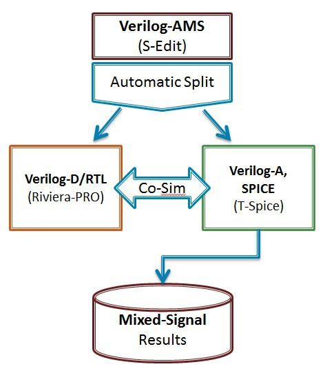
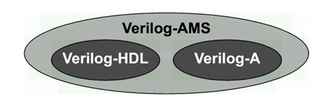
Verilog-AMS Verilog-A介绍 最近浅学了一下Verilog-AMS和Verilog-A的语法,记录一下自己理解:.Verilog-A是Verilog-AMS的子集,Verilog-A是只对analog电路进行建模的(运行基于Spice仿真器),而Verilog-AMS则可以对mixed- signal电路进行建模,包括了数字Verilog和Veirlog-A的语法 (运行基于 AMS混合信号仿真器).对于Verilog-A来说,其端口都是电器属性的,即类似于你从Spice里看到的那些模型一样;.对于Verilog-AMS来说,可以有logic类型的数字端口输入,然后electrical类型的模拟端口输出等等;.Verilog-AMS/A 可以从行为级和电路级对电路进行建模,简化了对于系统电路仿真时的复杂性;veirlog-AMS/Verilog-A中的关键概念:.分立信号转化为连续的信号 (对于数字只有0,1两种状态,但转化为连续信号,0->1过程值也会存在);.事件发生来触发信号变化(基于添加时间戳)(需解决设置的变量在事件未触发之前的初值问题);.在Verilog-A中,要时刻考虑Vth的特性,注意基于Verilog-A的model写法!.事件触发原理:在连续仿真器中,在发生事件处放置一个时间标记,从而将离散的仿真连续化;.model概念,branch概念,testbench概念(类似于verilog);一些关键代码:0. Verilog-A的阈值电压检测标准代码 (基于反相器):module inverter(out, in):output out;input in;electrical out, in;integer d_in; analog begin @(cross(V(in) - 0.5*V(vdd))) //穿越阈值电压写法(event statement),作用是在这个点建立时间戳,方便仿真器进行捕捉,否则捕捉不到这里发生的突变 ; //空白行,不在event发生时执行特定命令 d_in = V(in) > 0.5*V(vdd); //建立方波 V(out) <+ transition(!d_in, 0, 10n)*V(vdd); //用transition进行smooth处理 end endmodule.Model DAC (关键:electrical digital input -> (Vth) -> integer -> electrical analog differential output)module dac (out_p, out_n, in, clock, enable, vdda, gnda); output out_p, out_n; electrical out_p, out_n; input [7:0] in; electrical [7:0] in; input clock; electrical clock; input enable; electrical enable; input vdda; electrical vdda; input gnda; electrical gnda; integer code, en; real value;genvar i; analog begin // convert the input to a signed integer on positive clock edge @(cross(V(clock) - V(vdda)/2), +1) begin code = 0; for (i = 0; i < 8; i = i + 1) begin @(cross(V(in[i]) - V(vdda)/2)); if (V(in[i]) > V(vdda)/2) code = code + (1 << i); if (code >= 128) code = code - 256; value = code/256.0; end // reset output value when disabled @(cross(V(enable) - V(vdda)/2)) ; if (V(enable) < V(vdda)/2) value = 0; // drive the differential output V(out_p) <+ V(vdda)/2 + transition(value/2, 0, 10n); V(out_n) <+ V(vdda)/2 - transition(value/2, 0, 10n); end endmodule2. Model ADC (关键:electrical analog input -> (vth) -> integer -> electrical digital output)module adc (out, in, clk); output [5:0] out; input in, clk; electrical [5:0] out; electrical in, clk; parameter real vh = 1; parameter real vth = vh/2; parameter real tt = 100n from (0:inf); integer result; genvar i; analog begin @(cross(V(clk) - vth, +1)) begin result = 64*(V(in)+1)/2; if (result > 63) result = 63; else if (result < 0) result = 0; end for (i=0; i<6; i=i+1) V(out[i]) <+ transition(result & (1<<i) ? vh : 0, 0, tt); end endmodule3. Model Multiplexer: (关键:[3:0] sel 可以直接放入 @()中)module(out, in, sel); output out; electrical out; input [3:0] in; electrical [3:0] in; input [3:0] sel; logic [3:0] sel; analog begin @(sel) ; V(out) <+ V(in[0])*transition(sel === 0, 0, 100n); V(out) <+ V(in[1])*transition(sel === 1, 0, 100n); V(out) <+ V(in[2])*transition(sel === 2, 0, 100n); V(out) <+ V(in[3])*transition(sel === 3, 0, 100n); end endmodule4. 对于Cadence语法限制的标准处理方法:(Unfortunately, the Cadence simulator places unreasonable restrictions on event expressions in the analog block. Specifically, any digital signals used in an analog event expression must be preceded by either the posedge or negedge qualifiers. Thus, the model must be modified when intended for the Cadence simulator: )module cp (out, u, d): output out; electrical out; input u, d; logic u, d; reg sync = 0; always @(u or d) sync <= !sync; analog begin @(posedge sync or negedge sync) ; I(out) <+ 10u*(transition(d, 0, 1n) - transition(u, 0, 1n)); end endmodulean example of writing in Cadence:Cadence’s AMS simulator only supports discrete transitions filtered through posedge or negedge. Putting a discrete wire, discrete variable, or named event directly in a continuous event statement is not supported (as of 2014).real vgain;always @(gain) vgain = pow(10, (gain - 32.0)/20); real voffset;always @(offset) voffset = 1m*offset; reg break = 0;always @(vgain or voffset or en) break <= break; analog begin @(posedge break or negedge break) ; V(out) <+ transition(en ? vgain : 0, 0, 100n) * V(in) + voffset; endWith Cadence’s simulator, you can use the following for modeling multiplexers:module(out, in, sel); output out; electrical out; input [3:0] in; electrical [3:0] in; input [3:0] sel; logic [3:0] sel; reg sync = 0; always @(sel) sync <= !sync; analog begin @(posedge sync or negedge sync) ; V(out) <+ V(in[0])*transition(sel === 0, 0, 100n); V(out) <+ V(in[1])*transition(sel === 1, 0, 100n); V(out) <+ V(in[2])*transition(sel === 2, 0, 100n); V(out) <+ V(in[3])*transition(sel === 3, 0, 100n); end endmoduleTo implement a Verilog-A version of a multiplexer:module(out, in, sel); output out; electrical out; input [3:0] in; electrical [3:0] in; input [3:0] sel; logic [3:0] sel; parameter real vdd = 2.5; integer SEL; genvar i; analog begin // convert the input to an integer SEL = 0; for (i = 0; i < 2; i = i + 1) begin @(cross(V(sel[i]) - vdd/2)); if (V(sel[i]) > vdd/2) SEL = SEL + (1 << i); end V(out) <+ V(in[0])*transition(SEL == 0, 0, 100n); V(out) <+ V(in[1])*transition(SEL == 1, 0, 100n); V(out) <+ V(in[2])*transition(SEL == 2, 0, 100n); V(out) <+ V(in[3])*transition(SEL == 3, 0, 100n); end endmodule