
搜索到
1
篇与
的结果
-
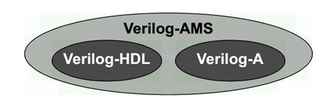
 Verilog-AMS Verilog-A介绍 最近浅学了一下Verilog-AMS和Verilog-A的语法,记录一下自己理解:.Verilog-A是Verilog-AMS的子集,Verilog-A是只对analog电路进行建模的(运行基于Spice仿真器),而Verilog-AMS则可以对mixed- signal电路进行建模,包括了数字Verilog和Veirlog-A的语法 (运行基于 AMS混合信号仿真器).对于Verilog-A来说,其端口都是电器属性的,即类似于你从Spice里看到的那些模型一样;.对于Verilog-AMS来说,可以有logic类型的数字端口输入,然后electrical类型的模拟端口输出等等;.Verilog-AMS/A 可以从行为级和电路级对电路进行建模,简化了对于系统电路仿真时的复杂性;veirlog-AMS/Verilog-A中的关键概念:.分立信号转化为连续的信号 (对于数字只有0,1两种状态,但转化为连续信号,0->1过程值也会存在);.事件发生来触发信号变化(基于添加时间戳)(需解决设置的变量在事件未触发之前的初值问题);.在Verilog-A中,要时刻考虑Vth的特性,注意基于Verilog-A的model写法!.事件触发原理:在连续仿真器中,在发生事件处放置一个时间标记,从而将离散的仿真连续化;.model概念,branch概念,testbench概念(类似于verilog);一些关键代码:0. Verilog-A的阈值电压检测标准代码 (基于反相器):module inverter(out, in):output out;input in;electrical out, in;integer d_in; analog begin @(cross(V(in) - 0.5*V(vdd))) //穿越阈值电压写法(event statement),作用是在这个点建立时间戳,方便仿真器进行捕捉,否则捕捉不到这里发生的突变 ; //空白行,不在event发生时执行特定命令 d_in = V(in) > 0.5*V(vdd); //建立方波 V(out) <+ transition(!d_in, 0, 10n)*V(vdd); //用transition进行smooth处理 end endmodule.Model DAC (关键:electrical digital input -> (Vth) -> integer -> electrical analog differential output)module dac (out_p, out_n, in, clock, enable, vdda, gnda); output out_p, out_n; electrical out_p, out_n; input [7:0] in; electrical [7:0] in; input clock; electrical clock; input enable; electrical enable; input vdda; electrical vdda; input gnda; electrical gnda; integer code, en; real value;genvar i; analog begin // convert the input to a signed integer on positive clock edge @(cross(V(clock) - V(vdda)/2), +1) begin code = 0; for (i = 0; i < 8; i = i + 1) begin @(cross(V(in[i]) - V(vdda)/2)); if (V(in[i]) > V(vdda)/2) code = code + (1 << i); if (code >= 128) code = code - 256; value = code/256.0; end // reset output value when disabled @(cross(V(enable) - V(vdda)/2)) ; if (V(enable) < V(vdda)/2) value = 0; // drive the differential output V(out_p) <+ V(vdda)/2 + transition(value/2, 0, 10n); V(out_n) <+ V(vdda)/2 - transition(value/2, 0, 10n); end endmodule2. Model ADC (关键:electrical analog input -> (vth) -> integer -> electrical digital output)module adc (out, in, clk); output [5:0] out; input in, clk; electrical [5:0] out; electrical in, clk; parameter real vh = 1; parameter real vth = vh/2; parameter real tt = 100n from (0:inf); integer result; genvar i; analog begin @(cross(V(clk) - vth, +1)) begin result = 64*(V(in)+1)/2; if (result > 63) result = 63; else if (result < 0) result = 0; end for (i=0; i<6; i=i+1) V(out[i]) <+ transition(result & (1<<i) ? vh : 0, 0, tt); end endmodule3. Model Multiplexer: (关键:[3:0] sel 可以直接放入 @()中)module(out, in, sel); output out; electrical out; input [3:0] in; electrical [3:0] in; input [3:0] sel; logic [3:0] sel; analog begin @(sel) ; V(out) <+ V(in[0])*transition(sel === 0, 0, 100n); V(out) <+ V(in[1])*transition(sel === 1, 0, 100n); V(out) <+ V(in[2])*transition(sel === 2, 0, 100n); V(out) <+ V(in[3])*transition(sel === 3, 0, 100n); end endmodule4. 对于Cadence语法限制的标准处理方法:(Unfortunately, the Cadence simulator places unreasonable restrictions on event expressions in the analog block. Specifically, any digital signals used in an analog event expression must be preceded by either the posedge or negedge qualifiers. Thus, the model must be modified when intended for the Cadence simulator: )module cp (out, u, d): output out; electrical out; input u, d; logic u, d; reg sync = 0; always @(u or d) sync <= !sync; analog begin @(posedge sync or negedge sync) ; I(out) <+ 10u*(transition(d, 0, 1n) - transition(u, 0, 1n)); end endmodulean example of writing in Cadence:Cadence’s AMS simulator only supports discrete transitions filtered through posedge or negedge. Putting a discrete wire, discrete variable, or named event directly in a continuous event statement is not supported (as of 2014).real vgain;always @(gain) vgain = pow(10, (gain - 32.0)/20); real voffset;always @(offset) voffset = 1m*offset; reg break = 0;always @(vgain or voffset or en) break <= break; analog begin @(posedge break or negedge break) ; V(out) <+ transition(en ? vgain : 0, 0, 100n) * V(in) + voffset; endWith Cadence’s simulator, you can use the following for modeling multiplexers:module(out, in, sel); output out; electrical out; input [3:0] in; electrical [3:0] in; input [3:0] sel; logic [3:0] sel; reg sync = 0; always @(sel) sync <= !sync; analog begin @(posedge sync or negedge sync) ; V(out) <+ V(in[0])*transition(sel === 0, 0, 100n); V(out) <+ V(in[1])*transition(sel === 1, 0, 100n); V(out) <+ V(in[2])*transition(sel === 2, 0, 100n); V(out) <+ V(in[3])*transition(sel === 3, 0, 100n); end endmoduleTo implement a Verilog-A version of a multiplexer:module(out, in, sel); output out; electrical out; input [3:0] in; electrical [3:0] in; input [3:0] sel; logic [3:0] sel; parameter real vdd = 2.5; integer SEL; genvar i; analog begin // convert the input to an integer SEL = 0; for (i = 0; i < 2; i = i + 1) begin @(cross(V(sel[i]) - vdd/2)); if (V(sel[i]) > vdd/2) SEL = SEL + (1 << i); end V(out) <+ V(in[0])*transition(SEL == 0, 0, 100n); V(out) <+ V(in[1])*transition(SEL == 1, 0, 100n); V(out) <+ V(in[2])*transition(SEL == 2, 0, 100n); V(out) <+ V(in[3])*transition(SEL == 3, 0, 100n); end endmodule