
搜索到
15
篇与
的结果
-
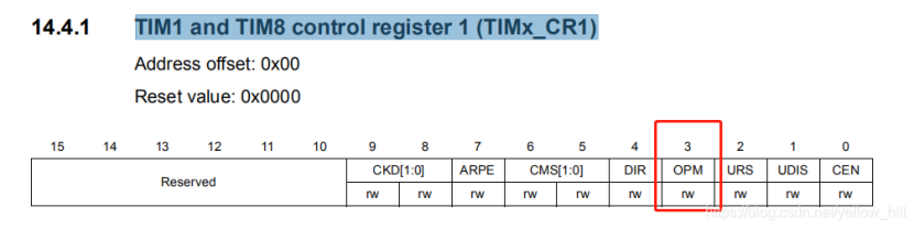
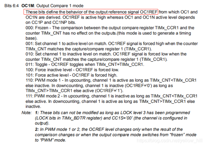
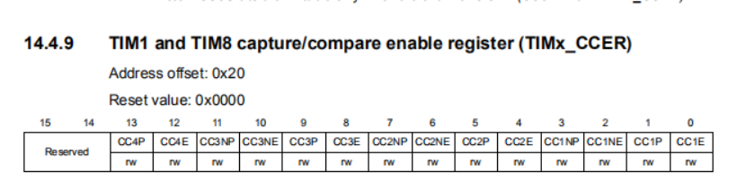
 STM32 - 定时器的设定 -高级- 08 - One-pulse mode - 触发波的实现 - 可变长度和相位 前言:直接开讲,请耐心看完 :首先,OPM模式的波形可以通过主从模式进行触发,其次,OPM模式的波形本身可以进行波形定制。1 OPM定义和功能说明One-pulse mode (OPM) is a particular case of the previous modes. It allows the counter to be started in response to a stimulus and to generate a pulse with a programmable length after a programmable delay.OPM 模式是一个比较特殊的模式,该模型的参数包括:可以定制的长度和Delay(相位)的波形Starting the counter can be controlled through the slave mode controller. Generating the waveform can be done in output compare mode or PWM mode.定时器的触发可以通过主从模式的定时器来控制,而输出波形可以是CC模式或者PWM模式。Select One-pulse mode by setting the OPM bit in the TIMx_CR1 register. This makes the counter stop automatically at the next update event UEV.在TIMx_CR1选择OPM模式使能OPM,同时定时器的计数器在下一个Event UEV停止计数2 OPM设定的定时器通道相关控制寄存器:2.1 OPM-使能-定时器控制寄存器:TIM1 and TIM8 control register 1 (TIMx_CR1)OPM模式,其实就是在一个脉冲波形后暂停计数,就这么简单,后面也方便你定制。Bit 3 OPM: One pulse mode0: Counter is not stopped at update event1: Counter stops counting at the next update event (clearing the bit CEN)2.2 OPM-波形的设定:使能OPM之后,后面就是对OPM的输出波形进行设置:波形的设定,用CC(捕捉比较)的方式, 就是用定时器的计数去比较你的各种设定,然后,各种翻转逻辑,最后实现波形的定制。A pulse can be correctly generated only if the compare value is different from the counter initial value.后面要做的事情就是CNT(counter的计数)和CCRx \ ARR进行比较,当然在比较之前,如下:Before starting (when the timer is waiting for the trigger), the configuration must be:(向上计数的时候)CNT的计数应该小于CCRX或 ARR这样才能产生波形。• In upcounting: CNT < CCRx ≤ ARR (in particular, 0 < CCRx)• In downcounting: CNT > CCRx2.2.1 设定输出波形的细节The OPM waveform is defined by writing the compare registers (taking into account the clock frequency and the counter prescaler).• The tDELAY is defined by the value written in the TIMx_CCR1 register.我们知道CCR为CC模式的比较值,这个值来决定Delay也就是相位• The tPULSE is defined by the difference between the auto-reload value and the compare value (TIMx_ARR - TIMx_CCR1).自动装载值和比较值之间的差值用了决定脉宽• Let us say the user wants to build a waveform with a transition from ‘0’ to ‘1’ when a compare match occurs and a transition from ‘1’ to ‘0’ when the counter reaches the auto-reload value.我们假设我们的波形在CC模式比较匹配时候为高电平翻转,而当定时器计数达到自动装载值的时候为低电平翻转。所谓CC模式比较匹配,就是CNT = CCRx,这时候电平翻转到高,定时器计数达到自动装载值,就是CNT = ARR的时候,高电平变成低电平下图做了一些修改,原图遗失CCR1的横坐标线对于输出的波形有多种选择,To do this, enable PWM mode 2 by writing OC1M=111 in the TIMx_CCMR1 register.111: PWM mode 2 - In upcounting, channel 1is inactive aslongas TIMx_CNTelse active. In downcounting, channel 1is active aslongas TIMx_CNT>TIMx_CCR1 elseinactive.The user can optionally enable the preload registers by writing OC1PE=’1’ in the TIMx_CCMR1 register and ARPE in the TIMx_CR1 register.Bit 3 OC1PE: Output Compare1 preload enable0: Preload register on TIMx_CCR1 disabled. TIMx_CCR1 can be written at anytime, the new value is taken in account immediately.1: Preload register on TIMx_CCR1 enabled. Read/Write operations access the preload register. TIMx_CCR1 preload value is loaded in the active register at each update event.Bit 7 ARPE: Auto-reload preload enable0: TIMx_ARR register isnot buffered1: TIMx_ARR register is bufferedIn this case the compare value must be written in the TIMx_CCR1 register, the auto-reload value in the TIMx_ARR register, generate an update by setting the UG bit and wait for external trigger event on TI2.(STM32手册这里好像有错误,应该是CC2P,不是CC1P)CC2P is written to ‘0’ in this example.In our example, the DIR and CMS bits in the TIMx_CR1 register should be low.Bits 6:5 CMS[1:0]: Center-aligned mode selection 00: Edge-aligned mode. The counter counts up or down depending on the direction bit (DIR).Bit 4 DIR: Direction 0: Counter used as upcounterThe user only wants one pulse (Single mode), so '1’ must be written in the OPM bit in the TIMx_CR1 register to stop the counter at the next update event (when the counter rolls over from the auto-reload value back to 0). When OPM bit in the TIMx_CR1 register is set to '0', so the Repetitive Mode is selected. Particular case: OCx fast enable:OPM模式也可以转成多波复制的模式,只需要OPM 位设为0即可。In One-pulse mode, the edge detection on TIx input set the CEN bit which enables the counter. Then the comparison between the counter and the compare value makes the output toggle. But several clock cycles are needed for these operations and it limits the minimum delay tDELAY min we can get.局限性:就是Delay的最小时间是系统局限的,因为上述信号接入需要一点时间:If the user wants to output a waveform with the minimum delay, the OCxFE bit in the TIMx_CCMRx register must be set. Then OCxRef (and OCx) are forced in response to the stimulus, without taking in account the comparison. Its new level is the same as if a compare match had occurred. OCxFE acts only if the channel is configured in PWM1 or PWM2 mode.注意:要立即响应的得到最小Delay的话,需要使能OCXFE位,改位用来强制OCx对OCXREF的响应加速。这个代价换来的意义是,多了仅仅两个时钟周期的响应时间。For example the user may want to generate a positive pulse on OC1 (输出比较)with a length of tPULSE and after a delay of tDELAY as soon as a positive edge is detected on the TI2 input pin.2.3 设置触发和时钟通道,定时器信号通道选择:Let’s use TI2FP2 as trigger 1:选择触发信号:下图为Timer channel的图我们这样理解定时器通道,定时器通道分成两个部分:输入、输出输入的部分我们看:TI1 、TI2这些都是input,输入通道包括输入滤波(可以滤除小的脉冲)和边沿检测,这样就到了TIxFPx(也就是输入经过滤波和预分频检测后的波形,叫做TI2FP2 Filtered Timer2 Input 2)。然后是,IC1,input capture输入捕捉通道,也属于输入吧,这里又有在预分频后的信号叫,ICx,(每个信号给他定一个名称就是为了后面负责的通道组合做好标识)。然后是,OC,输出比较通道,现在开始算输出通道。在进入输出通道OC之前,要开始做复杂的波形运算,达到我们想要的波形。就必须通过捕捉比较寄存器。通过设定通道的OCXREF、DTG的给到输出通道。• Map TI2FP2 to TI2 by writing CC2S=’01’ in the TIMx_CCMR1 register.将定时器输入通道TI2连接到TI2FP2,实际上是启用了CH2,将通道设定之后,通道的输出也就设定好了。• TI2FP2 must detect a rising edge, write CC2P=’0’ in the TIMx_CCER register.Bit 1 CC1P: Capture/Compare 1 output polarityCC1 channel configured as output:0: OC1 active high1: OC1 active low• Configure TI2FP2 as trigger for the slave mode controller (TRGI) by writing TS=’110’ in the TIMx_SMCR register.准备将TI2FP2作为从控制器的输入:TIM1 and TIM8 slave mode control register (TIMx_SMCR)Bits 6:4 TS[2:0]: Trigger selectionThis bit-field selects the trigger input to be used to synchronize the counter.000: Internal Trigger 0 (ITR0)001: Internal Trigger 1 (ITR1)010: Internal Trigger 2 (ITR2)011: Internal Trigger 3 (ITR3)100: TI1 Edge Detector (TI1F_ED)101: Filtered Timer Input 1 (TI1FP1)110: Filtered Timer Input 2 (TI2FP2)111: External Trigger input (ETRF)• TI2FP2 is used to start the counter by writing SMS to ‘110’ in the TIMx_SMCR register (trigger mode).Bits 2:0 SMS: Slave mode selectionWhen external signals are selected the active edge of the trigger signal (TRGI) is linked to the polarity selected on the external input (see Input Control register and Control Register description.000: Slave mode disabled - if CEN = ‘1’ then the prescaler is clocked directly by the internal clock.001: Encoder mode 1 - Counter counts up/down on TI2FP1 edge depending on TI1FP2 level.010: Encoder mode 2 - Counter counts up/down on TI1FP2 edge depending on TI2FP1 level.011: Encoder mode 3 - Counter counts up/down on both TI1FP1 and TI2FP2 edges depending on the level of the other input.100: Reset Mode - Rising edge of the selected trigger input (TRGI) reinitializes the counter and generates an update of the registers.101: Gated Mode - The counter clock is enabled when the trigger input (TRGI) is high. The counter stops (but is not reset) as soon as the trigger becomes low. Both start and stop of the counter are controlled.110: Trigger Mode - The counter starts at a rising edge of the trigger TRGI (but it is not reset). Only the start of the counter is controlled.111: External Clock Mode 1 - Rising edges of the selected trigger (TRGI) clock the counter.最后,来一个重点中的重点,相位调节示意图:摘自csdn有道云笔记2021-11-16 16:21:47
 -
STM32 - 定时器的设定 - 基础- 07 - 6-step PWM generation - 6步长PWM的产生 - COM Event的解释 前言:本节主要讲互补输出的步长设定问题,同时引入了一个重要的参数COM,这个再诸多STM32的手册里面都过于分散,在本文有一个比较完备的小结: When complementary outputs are used on a channel, preload bits are available on the OCxM, CCxE and CCxNE bits.互补输出主要由以下三个可以预设的设定决定:1 OC1M,OC1通道的输出模式,首先有OC1REF的模式决定,OC1REF会接到OC1 、OC1N然后,在OC1这里进行第二次设置,这里的设置又包括比较复杂的一组设定,有一个表:COM:(COM COMMUTATION交换 EVENT)or (Capture/Compare control update)COM的引入:提到COM之前,我们先看:定时器的控制寄存器2,里面的CCPC,CCUS控制位TIM1 and TIM8 control register 2 (TIMx_CR2)这里控制寄存器的CCPC位,决定了CCP 的 Preloaded的使能,这里定义了COM的2种出现的形式:(COMG bit set or rising edge detected on TRGI, depending on the CCUS bit).而CCUS里面的定义,则是对上述使能做更新的选择:事件产生寄存器TIM1 and TIM8 event generation register (TIMx_EGR)也就是COMGBit 5 COMG: Capture/Compare control update generation1: When CCPC bit is set, it allows to update CCxE, CCxNE and OCxM bitsCCPC预设值使能后,COM的相关使能位可以通过预设先设定好,而这三个通道恰恰就是决定了互补的输出波形,这些预设值在COM的EVENT的时候给到实际的shadow寄存器。The preload bits are transferred to the shadow bits at the COM commutation event. The user can thus program in advance (提前预设)the configuration for the next step and change the configuration of all the channels at the same time.COM can be generated by software by setting the COM bit in the TIMx_EGR register or by hardware (on TRGI rising edge).COM 的EVENT设定值可以是软件设定TIMx_EGR来实现,也可以 由硬件上升沿触发决定。EVENT发生的时候,会更新状态寄存器A flag is set when the COM event occurs (COMIF bit in the TIMx_SR register),Bit 5 COMIF: COM interrupt flagThis flag is set by hardware on COM event (when Capture/compare Control bits - CCxE, CCxNE, OCxM - have been updated). It is cleared by software.0: No COM event occurred.1: COM interrupt pending. 同时也可以产生中断:which can generate an interrupt (if the COMIE bit is set in the TIMx_DIER register) or a DMA request(if the COMDE bit is set in the TIMx_DIER register).Bit 5 COMIE: COM interrupt enable0: COM interrupt disabled1: COM interrupt enabledFigure 91 describes the behavior of the OCx and OCxN outputs when a COM event occurs,in 3 different examples of programmed configurations.Example 1:1 CO1M = 100 : OC1REF 为低电平 预设值2 CC1NE = 0, 那么 OCXN 的互补输出被关闭了3 CC1E = 1,OC1 的输出依据OCXREF的输出,再结合MIX的Table组合:当COM = 1 ,也就是,TIMx_EGR 的 COMG 更新的时候COM EVENT 事件产生,同时更新设置,那么OC1REF force low,OC1的输出被拉倒低电平Example 2:和例子1不同的是,CC1NE的值设为1,这样互补通道打开,同时OC1M设为1,那么OC1REF 被Force to High 给到OC1如果之前OC1REF就是高,那么他是不变的,互补输出通道则由原来的LOW改为和OC1REF一致为高,所有的这些变动,都是在COM TO 1的时候生效,这个和SAMPLE1 一致,仔细看这个例子,前面互补输出的通道都是正常的,到COM TO 1 触发之后,OC1N的通道就一直未低电平了,DISABLE。该例子给出了OC1REF的两个互补波形,而且还带死区的Delay有道云笔记2021-11-16 15:30:49
-
STM32 - 高级定时器的设定 - 基础-05 - 输出波形控制 The advanced-control timers (TIM1 and TIM8) can output two complementary(互补) signals and manage the switching-off and the switching-on instants of the outputs. This time is generally known as dead-time and it has to be adjust it depending on the devices connected to the outputs and their characteristics (intrinsic delays of level-shifters, delays due to power switches...)User can select the polarity of the outputs (main output OCx or complementary OCxN) independently for each output.This is done by writing to the CCxP and CCxNP bits in the TIMx_CCER register.TIMx_CCER 使能控制寄存器,控制CCxP 、CCxNP ,Bit 1 CC1P: Capture/Compare 1 output polarityCC1 channel configured as output:0: OC1 active high1: OC1 active lowBit 3 CC1NP: Capture/Compare 1 complementary output polarity0: OC1N active high.1: OC1N active low.The complementary signals OCx and OCxN are activated by a combination of several control bits:the CCxE and CCxNE bits in the TIMx_CCER registerOC/OCN输出使能控制Bit 0 CC1E: Capture/Compare 1 output enableCC1 channel configured as output:0: Off - OC1 is not active. OC1 level is then function of MOE, OSSI, OSSR, OIS1, OIS1N and CC1NE bits.1: On - OC1 signal is output on the corresponding output pin depending on MOE, OSSI, OSSR, OIS1, OIS1N and CC1NE bits.Bit 2 CC1NE: Capture/Compare 1 complementary output enable0: Off - OC1N is not active. OC1N level is then function of MOE, OSSI, OSSR, OIS1, OIS1N and CC1E bits.1: On - OC1N signal is output on the corresponding output pin depending on MOE, OSSI, OSSR, OIS1, OIS1N and CC1E bits.and the MOE, OISx, OISxN, OSSI and OSSR bits in the TIMx_BDTR TIM1 and TIM8 break and dead-time register (TIMx_BDTR)Bit 15 MOE: Main output enableThis bit is cleared asynchronously by hardware as soon as the break input is active. It is set by software or automatically depending on the AOE bit. It is acting only on the channels which are configured in output.0: OC and OCN outputs are disabled or forced to idle state.1: OC and OCN outputs are enabled if their respective enable bits are set (CCxE, CCxNE in TIMx_CCER register).See OC/OCN enable description for more details (Section 14.4.9: TIM1 and TIM8 capture/compare enable register (TIMx_CCER)).Bit 11 OSSR: Off-state selection for Run modeThis bit is used when MOE=1 on channels having a complementary output which are configured as outputs. OSSR is not implemented if no complementary output is implemented in the timer.See OC/OCN enable description for more details (Section 14.4.9: TIM1 and TIM8 capture/compare enable register (TIMx_CCER)).0: When inactive, OC/OCN outputs are disabled (OC/OCN enable output signal=0).1: When inactive, OC/OCN outputs are enabled with their inactive level as soon as CCxE=1or CCxNE=1. Then, OC/OCN enable output signal=1Bit 10 OSSI: Off-state selection for Idle modeThis bit is used when MOE=0 on channels configured as outputs.See OC/OCN enable description for more details (Section 14.4.9: TIM1 and TIM8 capture/compare enable register (TIMx_CCER)).0: When inactive, OC/OCN outputs are disabled (OC/OCN enable output signal=0).1: When inactive, OC/OCN outputs are forced first with their idle level as soon as CCxE=1 or CCxNE=1. OC/OCN enable output signal=1)Bits 7:0 DTG[7:0]: Dead-time generator setupThis bit-field defines the duration of the dead-time inserted between the complementary outputs. DT correspond to this duration.DTG[7:5]=0xx => DT=DTG[7:0]x tdtg with tdtg=tDTS.DTG[7:5]=10x => DT=(64+DTG[5:0])xtdtg with Tdtg=2xtDTS.DTG[7:5]=110 => DT=(32+DTG[4:0])xtdtg with Tdtg=8xtDTS.DTG[7:5]=111 => DT=(32+DTG[4:0])xtdtg with Tdtg=16xtDTS.Example if TDTS=125ns (8MHz), dead-time possible values are:0 to 15875 ns by 125 ns steps,16 us to 31750 ns by 250 ns steps,32 us to 63us by 1 us steps,64 us to 126 us by 2 us stepsand TIMx_CR2 registers.for more details. In particular, the dead-time is activated when switching to the IDLE state (MOE falling down to 0). Dead-time insertion is enabled by setting both CCxE and CCxNE bits, and the MOE bit if the break circuit is present. DTG[7:0] bits of the TIMx_BDTR register are used to control the dead-time generation for all channels.From a reference waveform OCxREF, it generates 2 outputs OCx and OCxN. If OCx and OCxN are active high:• The OCx output signal is the same as the reference signal except for the rising edge, which is delayed relative to the reference rising edge.(见下面分析)• The OCxN output signal is the opposite of the reference signal except for the rising edge, which is delayed relative to the reference falling edge.(见下面分析)If the delay is greater than the width of the active output (OCx or OCxN) then the corresponding pulse is not generated.The following figures show the relationships between the output signals of the dead-time generator and the reference signal OCxREF. (we suppose CCxP=0, CCxNP=0, MOE=1, CCxE=1 and CCxNE=1 in these examples)CC1P=0 ----> 0: OC1 active high CC1NP =0 ----> : 0: OC1N active high.MOE=1 ----> 1: OC and OCN outputs are enabledCCxE=1 ----> 1: On - OC1 signal is output on the corresponding output pin depending on MOE, OSSI, OSSR, OIS1, OIS1N and CC1NE bits.CCxNE=1 ----> 1: On - OC1N signal is output on the corresponding output pin depending on MOE, OSSI, OSSR, OIS1, OIS1N and CC1E bits.笔者案:我们现在依据上面的这个例子来分析一下:• The OCx output signal is the same as the reference signal except for the rising edge, which is delayed relative to the reference rising edge首先看OCX的输出,他应该是完全和OCXREF的输出一致,除了,上升沿会增加死区延时:蓝色为相同部分,后面上升沿往后移动了一格设定的delay时间。• The OCxN output signal is the opposite of the reference signal except for the rising edge, which is delayed relative to the reference falling edge.(见下面分析)The dead-time delay is the same for each of the channels and is programmable with the DTG bits in the TIMx_BDTR register.delay的时间通过DTG来控制。Re-directing OCxREF to OCx or OCxNIn output mode (forced, output compare or PWM), OCxREF can be re-directed to the OCx output or to OCxN output by configuring the CCxE and CCxNE bits in the TIMx_CCER register.将输出的OCXREF的波形可以转接到OCX 等其他端口,This allows the user to send a specific waveform (such as PWM or static active level) on one output while the complementary remains at its inactive level. Other possibilities are to have both outputs at inactive level or both outputs active and complementary with dead-time.Note: When only OCxN is enabled (CCxE=0, CCxNE=1), it is not complemented and becomes active as soon as OCxREF is high. For example, if CCxNP=0 then OCxN=OCxRef. On the other hand, when both OCx and OCxN are enabled CCxE=CCxNE=1) OCx becomes active when OCxREF is high whereas OCxN is complemented and becomes active whenOCxREF is low.有道云笔记2021-11-15 19:29:53
-
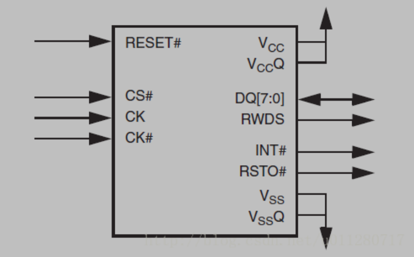
HyperBus Nor Flash小记 InterfaceMandatory I/O SummaryOptional I/O SummaryProtocal当HyperBus处于Idle状态(CK=Low & CK#=High)时,CS#从High变成Low,hyperbus的传输开始进行。最前面的三个时钟周期传输3个word的Command/Address(CA0, CA1, CA2),这三个word的CA用来决定这个传输一些特性。PS:这里面的word是2个byte,就是16bit。一个时钟周期是指两个clock,至于为什么这样定,我也不知道,Hyperbus的specification就是这么定的所以3个word的CA信息一共是48个bit。当传输完CA信息后,bus上需要传输一些dummy clock初始化RWDS信号。RWDS就是CK加了一些延迟的信号,用作高速读操作时的DQS。当数据传输开始,读数据是在RWDS的边沿进行采样,写数据是在Single-ended clock(即3.0V的CK)的边沿采样,或者在Differential clock(即1.8V CK和CK#)模式下,在CK和CK#交叉点进行数据采样。一旦完成数据传输,host就可以把CS#拉高并且把clock置为IDLE状态。当clock已经是IDLE状态了,拉嘎CS#就能结束一次传输。读时序下面贴出一个实际的读数据的时序, 读数据的地址是0x400。CA[48:0] = 0xA000004000。其中CA[47] = 1代表读,CA[46] = 0, CA[45] =1代表linear burst,ROW & Upper Column Address = 0x0000040 = 0x400 / 0x10, Lower Column Address=0x0 = 0x400 % 0x10。在插入了一些dummy的时钟周期后,进行了数据的采集。其中, 插入在CA和数据之间的dummy clock的个数是随设备不同而不同的,同时也跟Hyperbus的采样频率有关,这个需要参考不同的Hyberbus设备的手册才能知道。写时序写时序分为Write Transactions with Initial Latency和Write Transactions without Initial Latency。由于我并没有涉及太多的写设备的工作,所以这里就不多讲了。有Initial Latency的时序跟读时序差不多,只不过需要注意的是采样的时钟并不是RWDS即DQS,而是CK和CK#。而没有Initial Latency的就更简单了,直接数据就跟在CA后面,下面贴出官方Specification的是时序图。有道云笔记2021-11-08 11:34:45
-
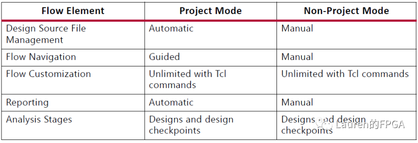
用Tcl实现Vivado设计全流程 Vivado有两种工作模式:project模式和non-project模式。这两种模式都可以借助VivadoIDE或Tcl命令来运行。相比之下,VivadoIDE给project模式提供了更多的好处,而Tcl命令使得non-project模式运行起来更简单。在project模式下,Vivado会自动管理整个设计流程和文件数据。最直接的体现是在Vivado左侧导航Flow Navigator下会显示所有流程,从设计输入到最终生成bit文件。同时,Vivado会自动创建相应的文件目录,生成相应的文件例如dcp以及相应的报告。Non-project模式是一种内存编译流程。用户可以从指定位置读取文件到内存中,然后进行编译。可以逐步执行每个步骤如综合、布局、布线等,可以根据需求设定编译参数。这一切都可以通过Tcl命令完成。显然,non-project模式下,用户可以通过Tcl命令管理设计文件和设计流程,体现了该模式的主要优势即用户对设计流程有完全的掌控力。Project模式和non-project模式的主要区别如下图所示。不难看出,project模式下更多的管理、操作都是“自动”完成的;而non-project模式下,则是“手工”完成的。从Tcl命令的角度而言,project和non-project模式也是不同的,如下图所示。Project模式下用到的Tcl命令是一种打包的命令,例如添加设计文件需用add_files,文件可以是HDL(包括VHDL,Verilog或SystemVerilog),可以是约束文件(包括.xdc或.tcl),可以是网表文件(可以是dcp,ngc或edif)等。Implementation时,命令launch_runs就可以按照指定的策略完成所有的步骤,包括生成相应的DCP。Non-project模式下用到的Tcl命令是分立的,例如,读入设计文件,如果是VHDL,需要用到read_vhdl;如果是Verilog,需要用到read_verilog,如果是.xdc,需要用到read_xdc;如果是DCP,需要用到read_checkpoint;如果是EDIF,需要用到read_edif。而在implementation时,需要分别用到opt_design、place_design、phys_opt_design和route_design等。因为Tcl命令使得non-project模式更能简单地运行,这里我们将介绍如何通过Tcl命令在non-project模式下完成所有步骤。有道云笔记2021-11-04 16:41:15